SPS(Semiconductor Package Substrate)
It is a core part in semiconductor packaging process, which is a high density board of fine circuit that connects semiconductor's electrical signal to the mainboard.
It is used for automotive and various mobile devices that require high reliability.


-
Overview
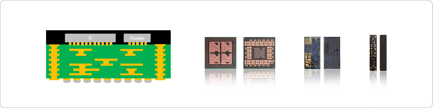
- SiP (System in Package)
- SiP is a product that implements multiple ICs and passive components within a substrate package to create a single system.
- It is used as a substrate for components related to RF (radio frequency), power, etc., in wearables and smartphones, requiring the substrate to have high reliability and tight specifications for signal transmission.
- Application
- RF SiP, Wifi, Bluetooth, IoT, Networking, PMIC, AiP
-
Core Technology
- Pattern Process : MSAP
- High Layer
- Coreless Technology
- Various Body Size (Small~Large)
- Layer to Layer Alignment
-
Specifications
HVM
(HVM Ready)Sample Layer & Thickness
(Coreless)3L 109µm ← 4L 110µm ← 5L 196µm ← 6L 192µm ← 7L (291µm) ← 8L (296µm) ← 9L (320µm) ← 10L (420µm) ← Via/Pad IVH
(≤40µm Core)50/90 50/85(± 17.5) BVH
(≤25µm PPG)50/80 40/65(± 12.5) Alignment (A/R less) ← Surface finish OSP(Tamura), Ni/Au+OSP, ENIG/ENENIG ← -
Product Image