SPS(Semiconductor Package Substrate)
It is a core part in semiconductor packaging process, which is a high density board of fine circuit that connects semiconductor's electrical signal to the mainboard.
It is used for automotive and various mobile devices that require high reliability.


-
Overview
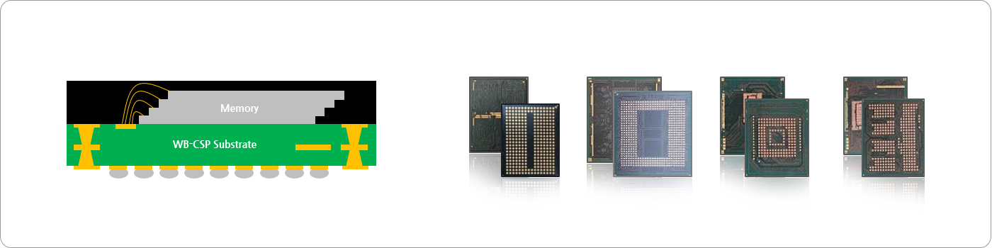
- WBCSP (Wire Bond Chip Scale Package)
- WBCSP connects the semiconductor chip to the substrate using gold wire, with the chip size occupying over 80% of the substrate area.
- Due to its capability for multi packaging via chip stack, it is widely used in memory chip packaging for mobile devices that demand miniaturization.
- Application
- Mobile Memory (LPDRAM/mobile NAND), NAND for SSD
-
Core Technology
- Pattern Process : Tenting, MSAP
- Thin Substrate
- Cored / Coreless
-
Specifications
HVM Sample Layer/Thickness/
CCL Thickness2L 100µm 40µm 94µm 30µm 3L 80µm (Coreless) 70µm (Coreless) 4L 120µm 35µm, 30µm 110µm 30µm Trace Pitch
(Width/Space)Tenting 50pt (25/25) ← MSAP 40pt (20/20) ← B/F Pitch
(Width/Space)Tenting 60pt (25/10) 50pt (20/10) MSAP 60pt (30/15)
55pt (25/15)50pt (25/10)
45pt (20/10)SR LPSR AUS308, AUS320 ← DFSR SR1, MG3, MG1_Z, AUS410, SR3 ← Material Low CTE, Low Stress ← -
Product Image