SPS(Semiconductor Package Substrate)
It is a core part in semiconductor packaging process, which is a high density board of fine circuit that connects semiconductor's electrical signal to the mainboard.
It is used for automotive and various mobile devices that require high reliability.


-
Overview
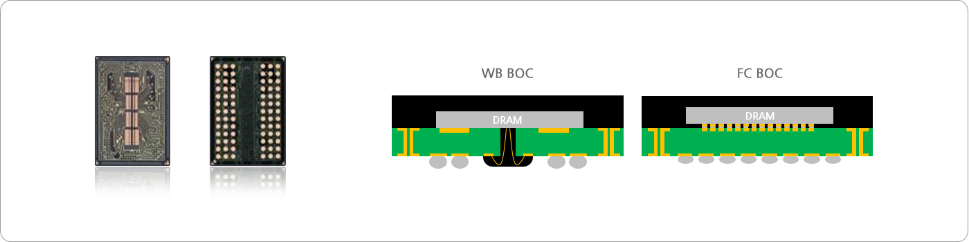
- BOC (Board on Chip)
- Since DDR2, substrate has been used instead of leadframe for packaging. At that time, due to the characteristic of chips being mounted face-down through a central slot, they were named Board on Chip, with wirebonding pads and solder balls being positioned on the same layer.
- Currently, there are WB BOC products that bond through slots as per the conventional method, and FC BOC products that directly connect chips to bump pads based on customer preferences.
- Application
- PC/Server/CXL Memory Module DRAM
-
Core Technology
- Pattern Process : Tenting, MSAP
-
Specifications
DDR4 DDR5 Layer 2L 2L Thickness 258~265µm 180~220µm Process Tenting Tenting, MSAP Trace Pitch (Width/Space) 55pt (25/30) 50pt (25/25) PSR AUS308 ← Surface Finish W/B Ni/Au ← F/C OSP ← -
Product Image